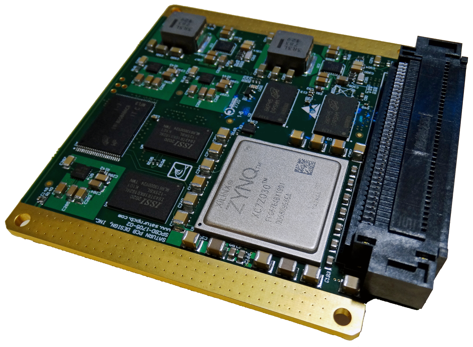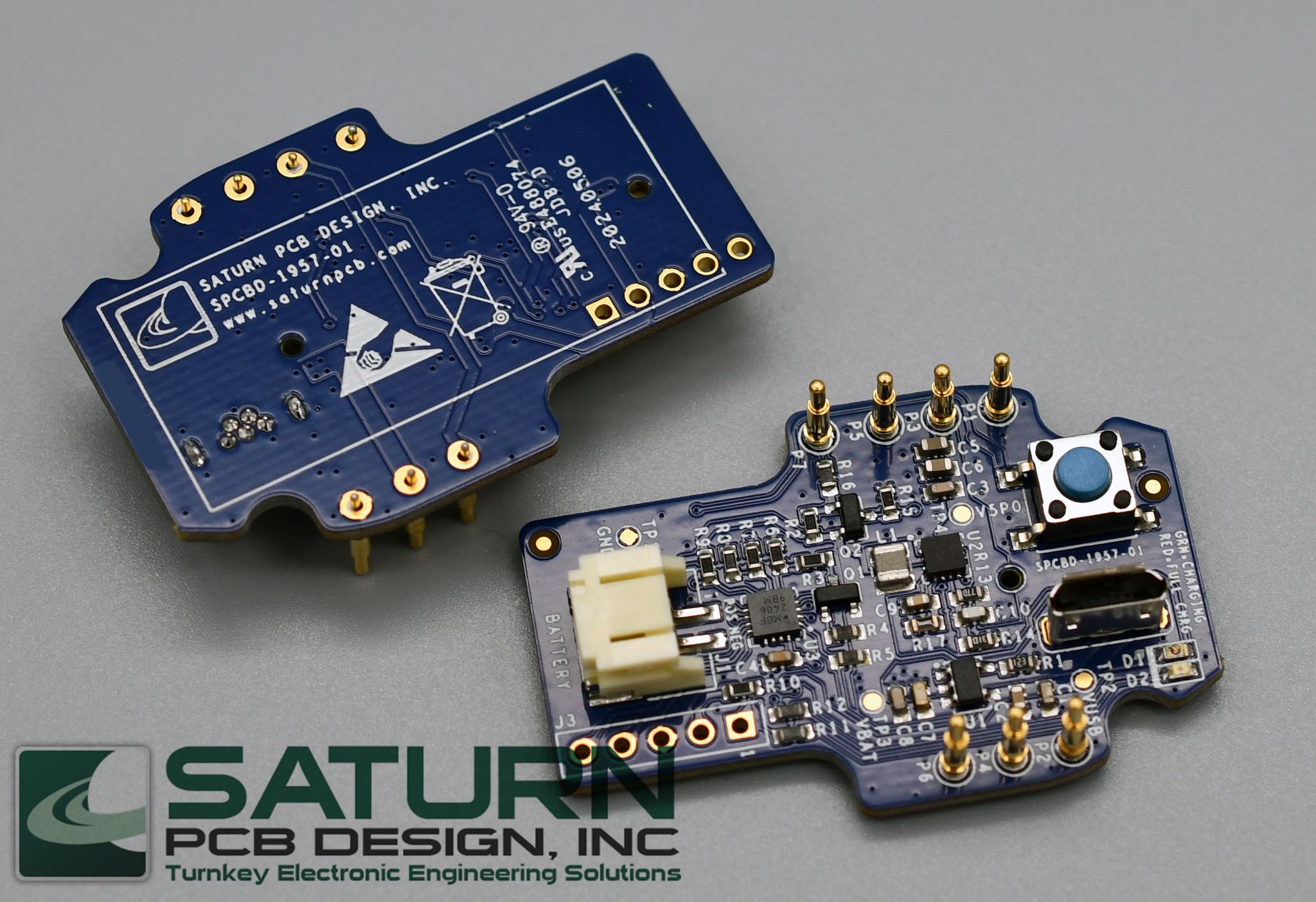
PCB Design Services
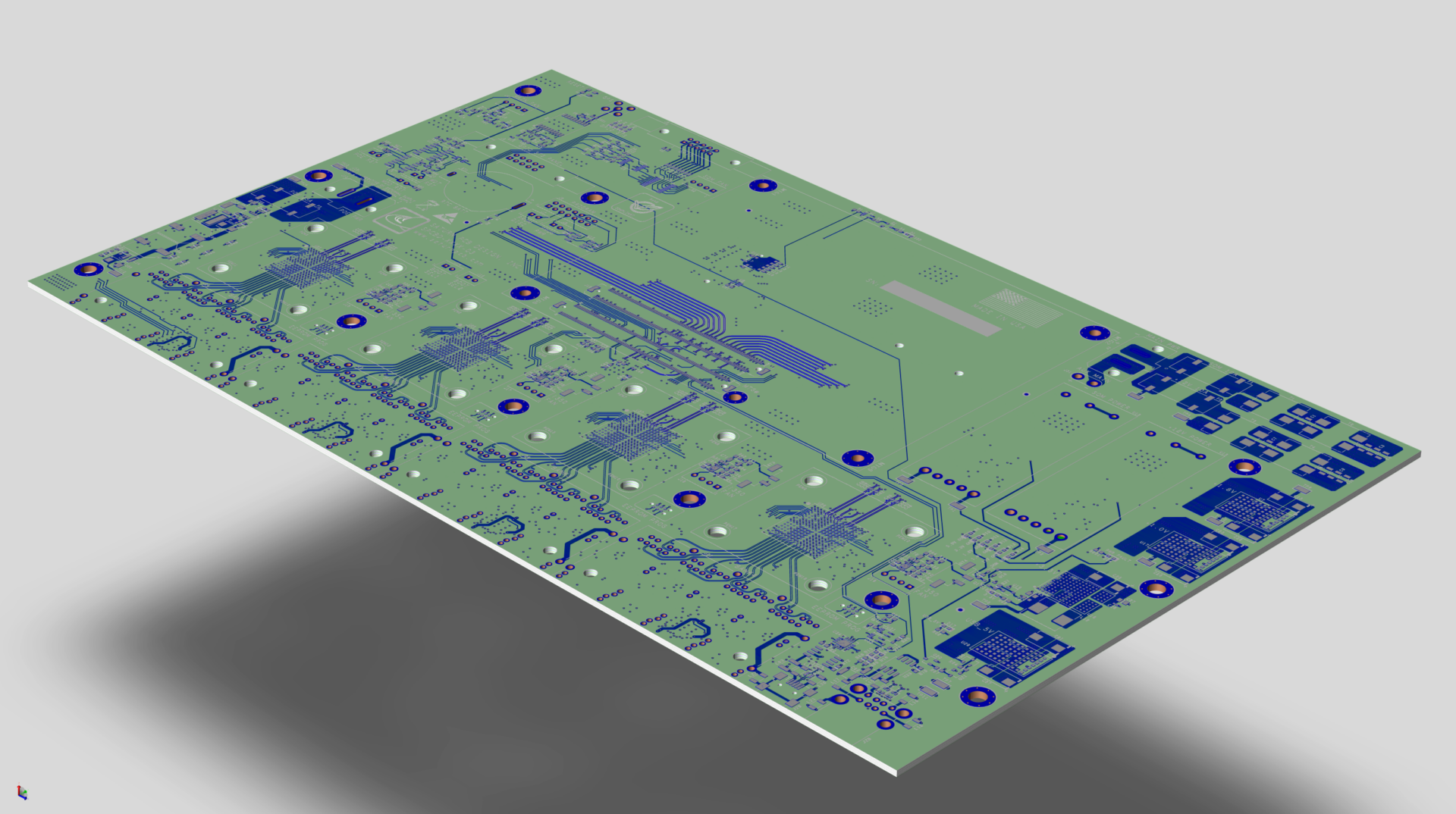
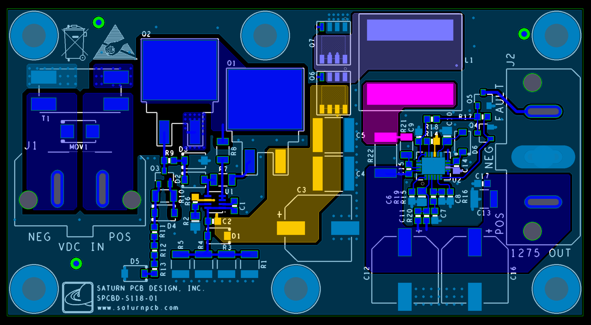
PCB design services are used to create the printed circuit boards that form the core of many electronic devices. Our PCB design services typically include schematic capture and design, PCB layout design, analyses to ensure manufacturability, testability, and signal integrity, and 3D modeling.
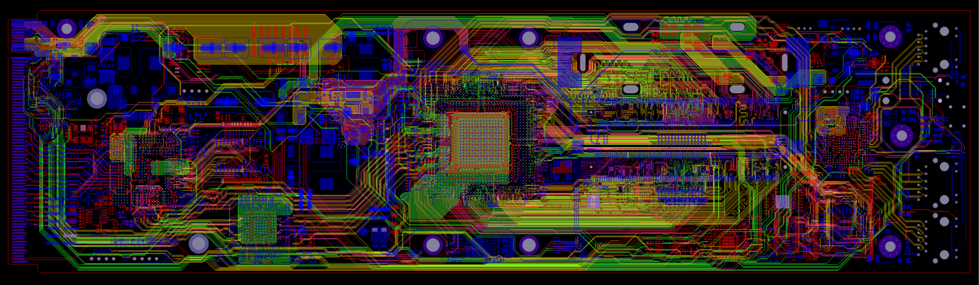
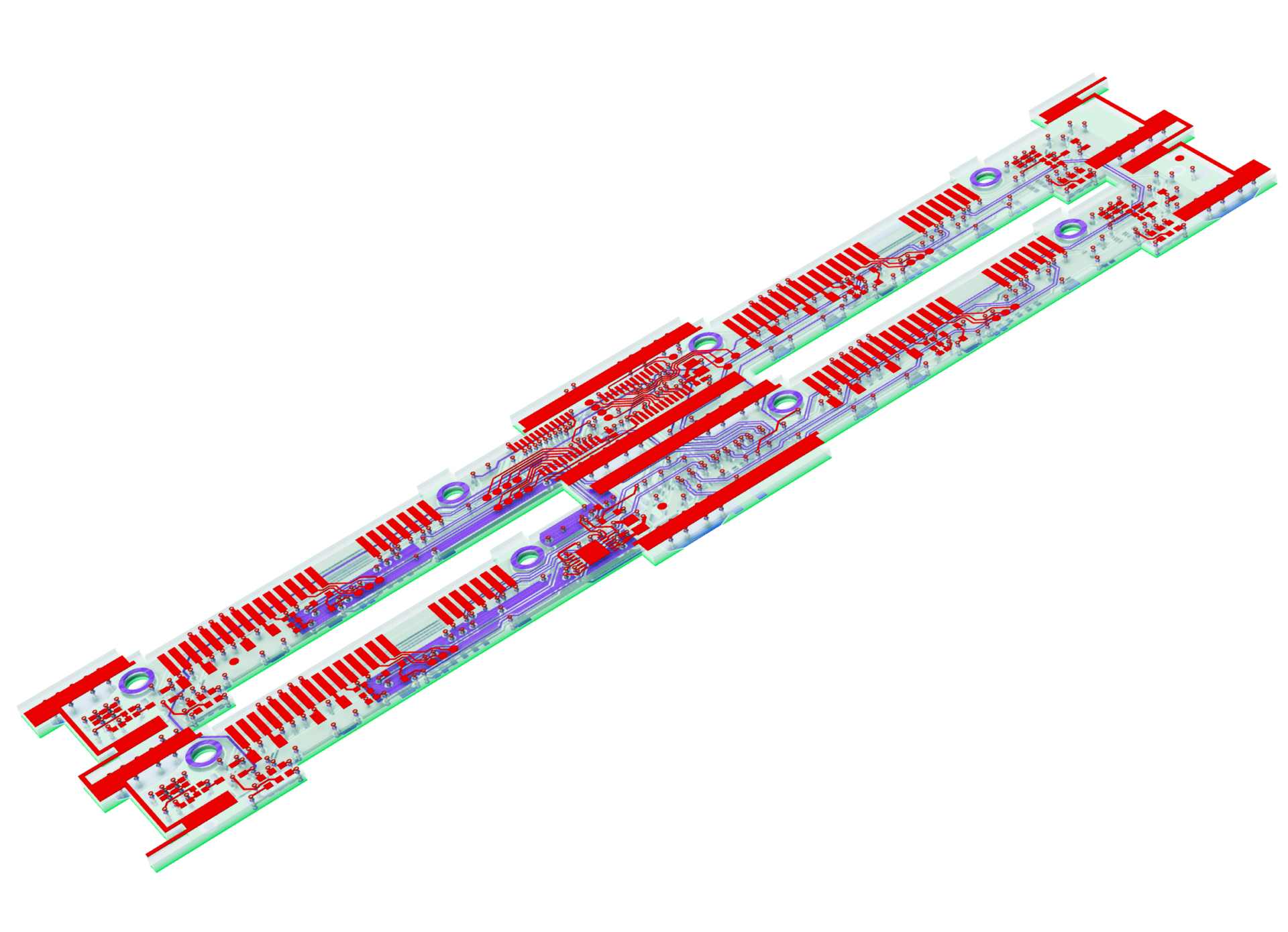
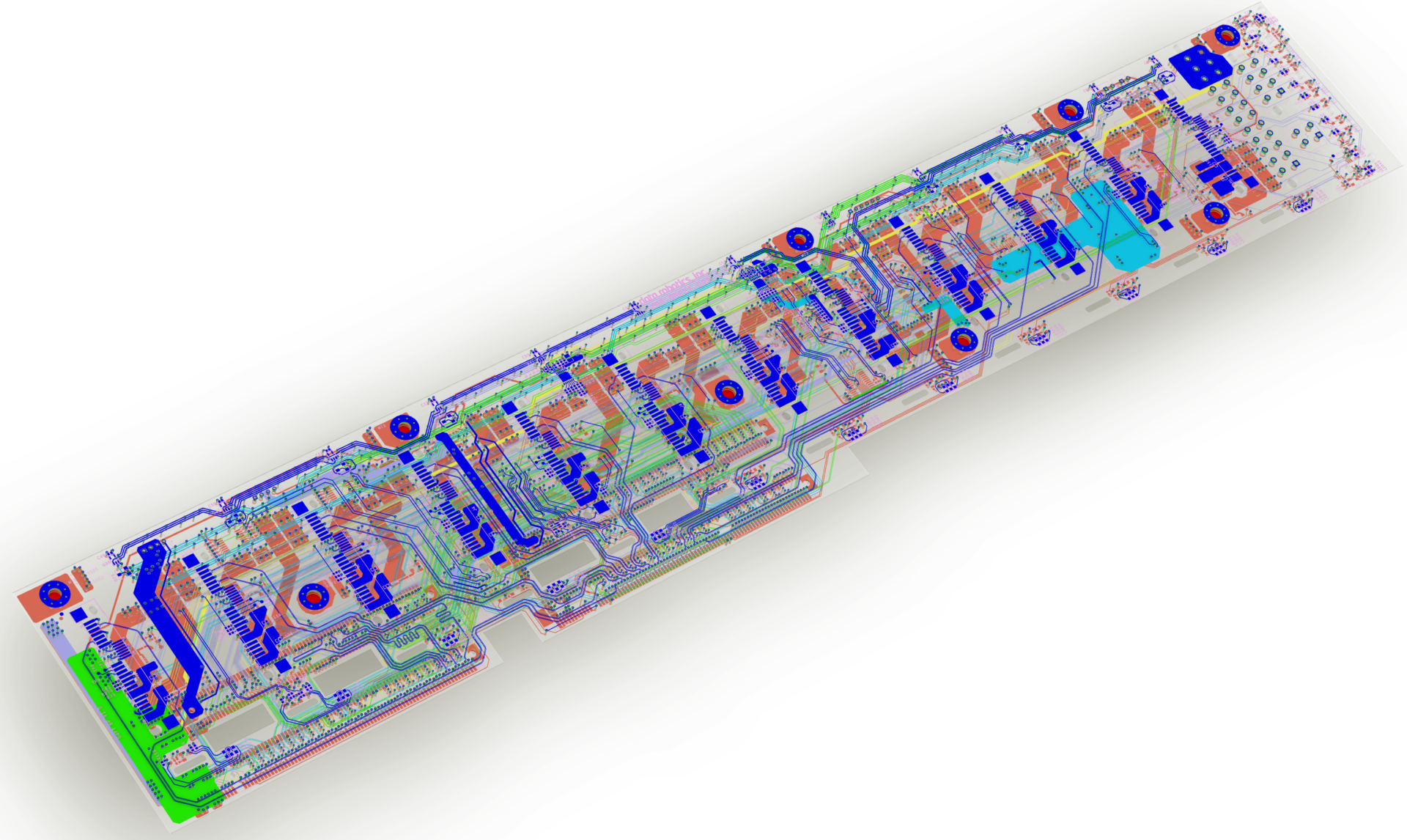
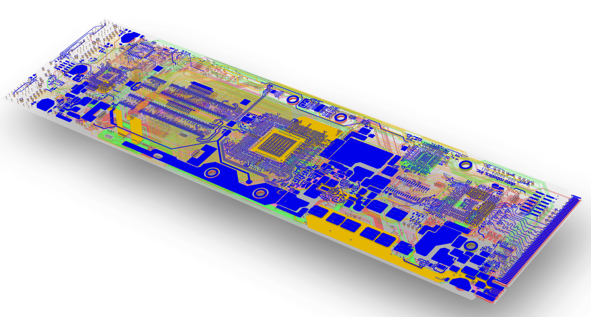
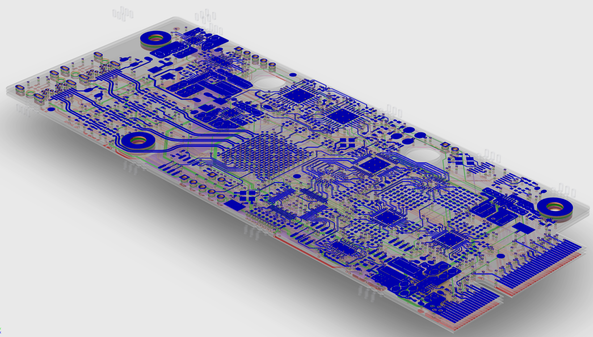
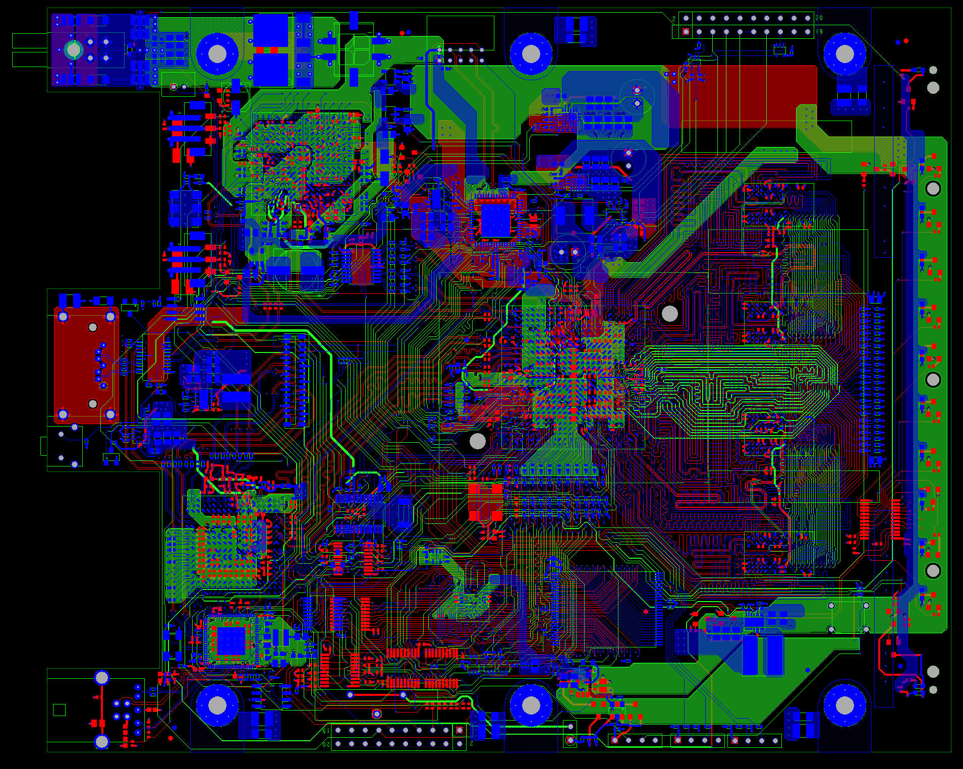
Design Capabilities
- HDI Designs with micro vias and advanced materials – Via-in-Pad, laser micro vias.
- High speed, multi layer digital PCB designs – Bus routing, differential pairs, matched lengths.
- PCB Designs for space, military, medical and commercial applications
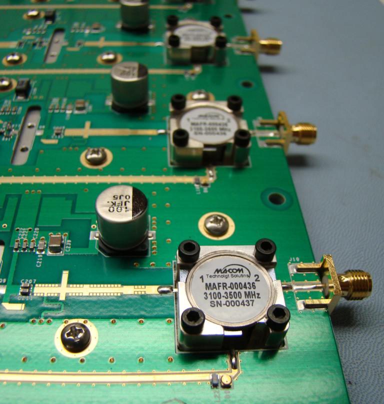
- Extensive RF and analog design experience (printed antennas, guard rings , RF shields…)
- Signal integrity issues to meet your digital design needs (tuned traces, diff pairs…)
- PCB Layer management for signal integrity and impedance control
- DDR2, DDR3, DDR4, SAS and differential pair routing expertise
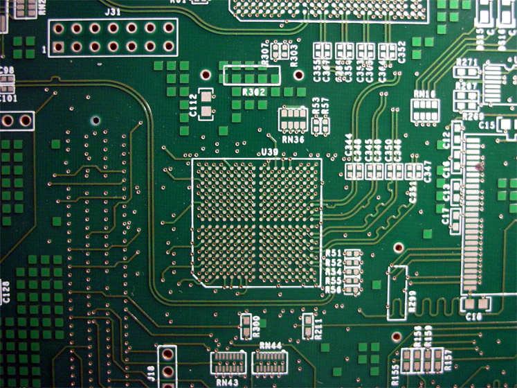
- High density SMT designs (BGA, uBGA, PCI, PCIE, CPCI…)
- Flex PCB designs of all types
- Low level analog PCB designs for metering
- Ultra low EMI designs for MRI applications
- Complete assembly drawings
- In-Circuit Test data generation (ICT)
- Drill, panel and cutout drawings designed
- Professional fabrication documents created
- Autorouting for dense PCB designs